Electron microscopy is quite different from optical
microscopy even if the images obtained appear very real and as
though illuminated naturally. The following is a simple
explanation for the interested layman. For further details,
please contact John
Donovan. (541) 346-4632
Scanning electron microscopy (SEM) or electron probe microanalysis (EPMA) are generally considered micro-analytical techniques which are able to image or analyze materials we can not generally observe with the resolution offered by visible techniques. By image we mean photograph an object much smaller than we can see, even with the aid of an optical microscope. The SEM has a unique capability of giving your view of a flea the same perspective as the Chevy in your driveway. By analyze we mean identify the elements (e.g., silicon, iron, etc) of which the specimen is composed. Elemental analysis can also be accomplished at a micro-scale; for example, EPMA can probe a specimen as small as 5 thousands of a millimeter (5 microns), and not only identify the elements present but measure them with a small degree of error. These instruments represent two if the greatest advances in scientific instrumentation, however they do have their limits. For example, not all specimens can be exposed to the high vacuum within the specimen chamber. Also, elements lighter than atomic number 8 (oxygen) can not be measured without reservations, and EPMA is not sensitive to many elements below 100ppm. Still, this instrumentation has proved invaluable, especially for mineralogists and petrologists, and a good operator can vary one parameter or another to circumvent instrumental weaknesses.
Courtesy of FEI Company, one can find a good introductory resource to scanning electron microscope concepts and terms here. Also a good page for general teaching resources on SEM is here.
These instruments belongs to a broad category of particle beam instruments. In this case we bombard materials with electrons which have high energies because they have mass and because they have been accelerated with tens of thousands of volts. Other particle beam instruments include ion probes (SIMS), proton probes (PIXA), and transmission electron microscopes (TEM). All particle beam instruments, while quite different in design, offer overlapping capabilities, and this is especially true of our instruments. Whereas SEMs have been historically used as cameras and microanalyzers used for elemental analysis, modern electron probes offer both capabilities while optimizing for one or the other. For example, our SEM can quantify x-rays with its energy dispersive x-ray detector (EDX), but it is designed for ease of use and for a variety of specimens. Our microprobe, on the other hand, is designed with its wave dispersive x-ray spectrometers (WDS) in mind and does not allow many freedoms, however EPMA can still image nearly as well as the SEM.
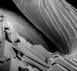
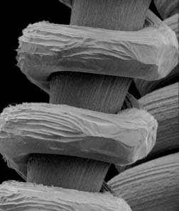 Scanning electron microscopes
have been generally used as cameras, that is, for photographing
specimens beyond the capabilities of ordinary optical
microscopes. While the images obtained appear very real and as if
they were photographed by ordinary means, the apparent
illumination is a function of particle emission rather than
radiation we're familiar with. These particles emitted are termed
secondary electrons, and their
detection via a SE detector is displayed on a scanning TV
display. A bright image will be the result of high secondary
electron emission, while the primary influence on high emission
is the surface structure of the specimen. The end result is
therefore brightness associated with surface characteristics and
an image which looks very much like a normally illuminated
subject.
Scanning electron microscopes
have been generally used as cameras, that is, for photographing
specimens beyond the capabilities of ordinary optical
microscopes. While the images obtained appear very real and as if
they were photographed by ordinary means, the apparent
illumination is a function of particle emission rather than
radiation we're familiar with. These particles emitted are termed
secondary electrons, and their
detection via a SE detector is displayed on a scanning TV
display. A bright image will be the result of high secondary
electron emission, while the primary influence on high emission
is the surface structure of the specimen. The end result is
therefore brightness associated with surface characteristics and
an image which looks very much like a normally illuminated
subject.
Electron probe microanalyzers are designed from the ground up for the analysis of x-rays which are emitted from the specimen when probed with an electron beam. The design considerations primarily accommodate three to six wave dispersive x-ray spectrometers which are inherently large. Specimens prepared for x-ray microanalysis are generally flat, and the microprobe analyzer is designed to allow only a considerable amount of x and y translation rather than the specimen manipulation which is typical of the SEM (for example, full rotation and tilt). The heart of EPMA is the wave dispersive technology (WDX) for detecting and counting x-rays. These spectrometers are much more sensitive to low elemental concentrations than are EDX detectors usually associated with SEM. Concentrations in the range of 500-1000ppm can generally be measured, and for some elements within some types of materials, the detection limit can be near 20ppm.
Like a radio which needs to be tuned to your favorite station's wavelength, these spectrometers need to be tuned to the wavelength of the element's characteristic x-ray. That is to say, if the measurement of 9 elements is desired (e.g., Si, Ti, Al, Fe, Mn, Mg, Ca, Na & K), then the tasks of counting their characteristic x-rays can be distributed across several spectrometers, with extended counting times for minor and trace elements-- thus, the requirement for more than one spectrometer.
The usefulness of quantifying elemental compositions is invaluable in the sciences of mineralogy, petrology and materials research. Students and investigators can measure the composition of several mineral phases which are, apparently or assumed, in equilibrium with each other. This information can be used to estimate the temperature and pressure at the time of crystallization. They are also able to measure the composition of a rock-forming mineral relative to its growth history; for example, its core and rim compositions. Material science applications are even more varied, from thin film semi-conductors to photonics materials to super conductors. In the case of thin-films, by measuring various x-ray intensities at a number of different accelerating voltages, both the composition and thickness of various films deposited on a substrate may be determined with excellent accuracy. Single crystal grown for various purposes can have their formula stoichiometry measured and compared with x-ray diffraction data.
All of these examples demonstrate EPMA's traditional use for
analyzing spot locations quantitatively.
Within the last decade, computer power and image analysis
software has allowed mapping of element distributions at various
scales. Here the researcher is interested in not only the
absolute elemental concentration, but also the spatial
distribution of elemental concentrations. New software and
hardware will allow elements to be qualitatively or
quantitatively mapped, over almost any area on a sample.
NEW!!
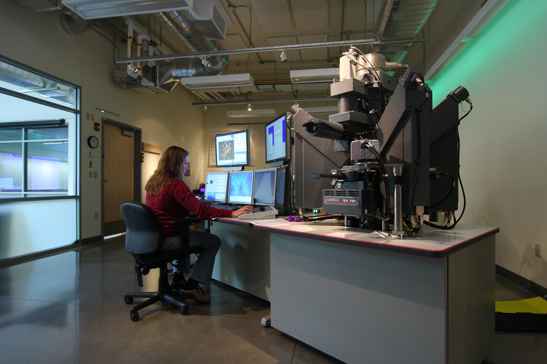
Our Cameca SX100 was installed in July 2005. It is a 5 spectrometer instrument (two four crystal spectrometers for simultaneous light element analysis and 3 large area crystals (1 LTAP, 1 LPET and 1 LLIF) for extended sensitivity) and catholuminescence. The SX100 has built in auto-focus and optical zoom capability. It has special multi-layer dispersive element "crystals" optimized for nitrogen and boron analysis. The instrument is completely digitally controlled from Windows XP. A Thermo-Electron EDS system has been ordered and will be installed early 2006 which will be integrated with the Probe for Windows software for full automation capability of WDS and EDS.
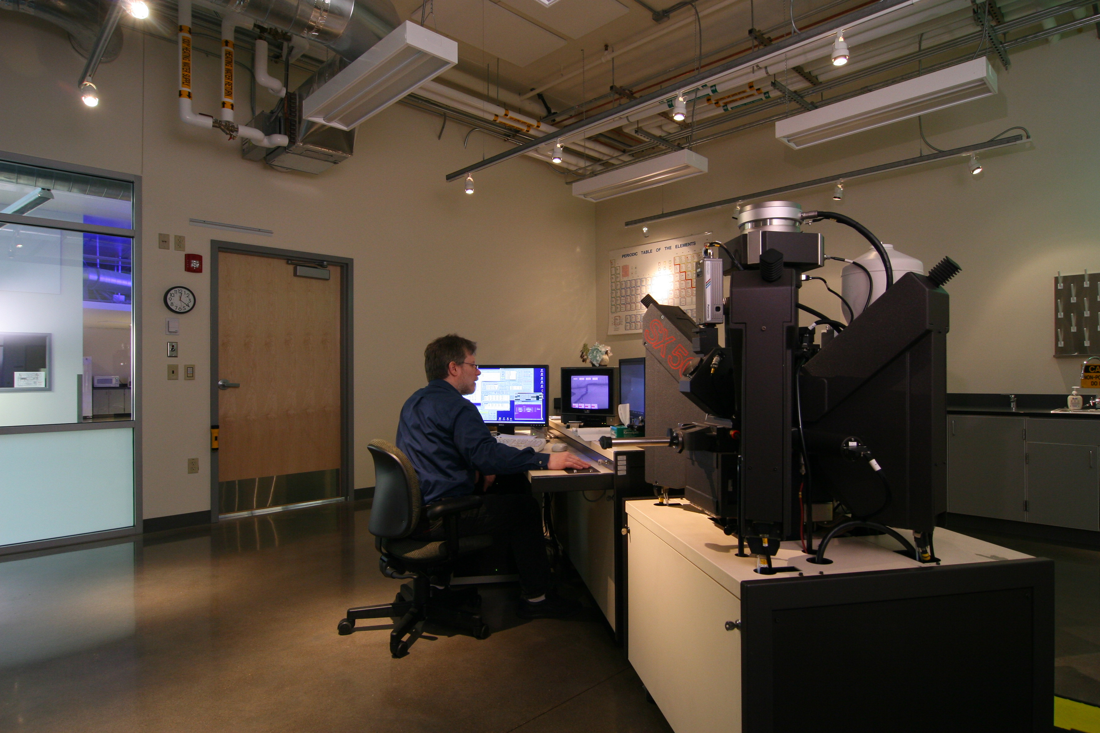
The SX50 was installed during the summer of 1989. It employs 4 vertical spectrometers, one of which is intended for light elemental analysis has 4 crystals (or x-ray reflectors), TAP, lead sterate, PC1 (fluorine, oxygen and carbon) and PC2 (boron). Our microprobe automation has been recently upgraded with the Probe for Windows (Enterprise Edition) software and hardware package commercially offered by Advanced Microbeam. This instrument was also upgraded with respect to its backscatter electron detector, therefore allowing excellent mineral grain imagery for selecting areas of interest for analysis.
The imaging capabilities have been further enhanced with a
digital frame store, which not only allows for much more
comfortable viewing, but digital image acquisition as well using
MicroImage digital acquisition software for analog (SE and BSE)
as well as x-ray mapping up to 4096 x 4096 pixel resolution.
NEW!!
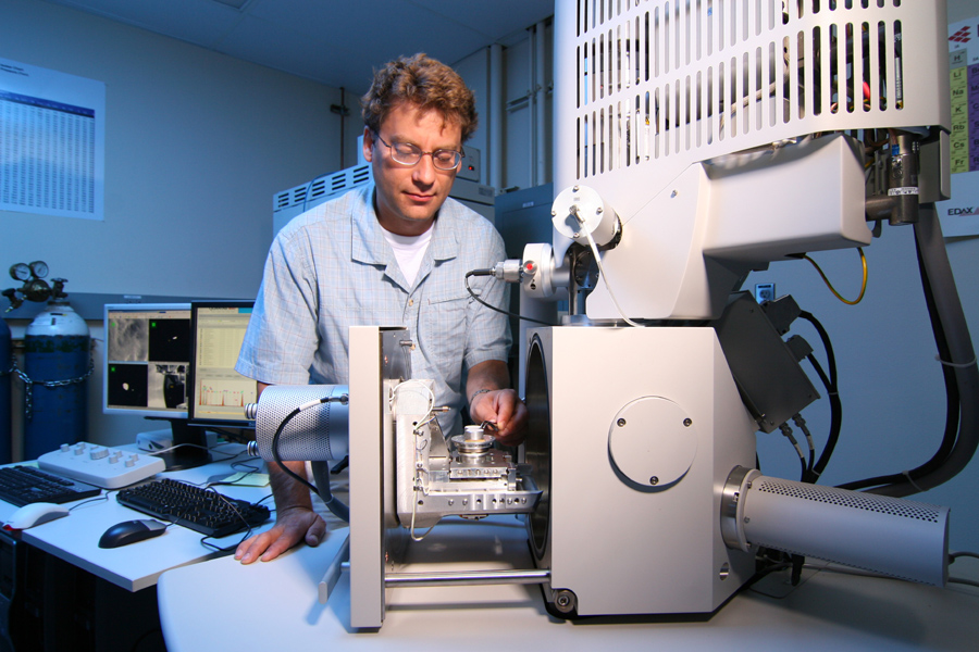
Our FEI Quanta 200 FEG scanning electron microscope (SEM) was installed in the summer of 2006. It is a high resolution environmental microscope capable of running in high vacuum, variable pressure and environmental modes which means that it can handle all specimens even uncoated, non-conductive samples as well as wet samples that require being above the vapor pressure of water. It has 3-5 nm resolution, high output thermal field emission (> 100nA beam current) microscope with a high sensitivity (18 mm) backscatter (BSE) detector for atomic number contrast. It also has a high speed SDD (silicon drift detector) for spectral imaging and phase analysis and an electron backscatter detection (EBSD) system for orientation imaging and texture mapping of crystalline and polycrystalline materials.
Traditionally SEM images are acquired by detecting the emission of secondary electrons. However this is only a small part of the information to be gained from the specimen due to its interaction with the primary electron beam. This facility's SEM also has the capability of detecting backscattered electrons (BSE) and electromagnetic radiation in the form of x-rays and normal light near the visible spectrum, i.e. cathodo-luminescence (CL). This particular instrument was also obtained for its ease of use at very low electron probe energies, which is very useful for imaging specimens that cannot be conductivity coated properly. Typical SEM electron probe voltages vary between 5keV and 40keV. This instrument, on the other hand, can be used easily near 100eV.
What sets this instrument apart from the electron
microprobe (EPMA) are the degrees of freedom the operator has
with instrumental parameters such as acceleration voltage, beam
current, final apertures and specimen manipulation, which
includes working distances between 5 and 48 mm, 360 degrees of
rotation and 80 degrees of tilt. The fact the operator is
unconstrained allows for the same creativity we all attribute to
photographic artists. The freedoms allowed within the specimen
chamber implies almost anything can be photographed with the
resolving power attributable to electron beam instruments.
Specimen preparation. This microanalytical
setting generally implies most of the specimens be flat and
polished. To this end, we offer within this facility two Struers
Rotopol-35 polishers, one set up for metallographic work and the
other for thin section work with an automated Multi-doser system.
Within this department are resources for preparing standard sized
and rectangular polished thin sections (contact Lori Suskin,
(541) 346-2835). Because this department generally examines
nonconductive specimens, it is a requirement they be coated with
a conductive material. An Edwards E306A and a Technics
Hummer III are available for carbon evaporation and noble
metal sputtering, respectively. Other than equipment, this
facility stocks a variety of consumables and almost anything for
handling or transferring specimens for EPMA and SEM.
Optical microscopy. This EPMA facility insists on
extensive optical evaluation such that electron probe projects,
or questions, are properly defined for efficient use of the
instrumentation, and several research grade optical microscopes
are available. These include: a Zeiss Photomicroscope for
incident and transmitted light microscopy, and 35mm
photomicrography; A Zeiss Axioskop with a Maerzhaeuser
digitizing stage for preselecting and storing points of interest;
and a variety of standard petrologic and stereo microscopes.
Computer resources. Controlling the Cameca microprobes and the FEI and Zeiss SEMs are dedicated computers for operation, automation and instrument-specific file storage. The Cameca SX50 EPMA utilizes a Windows 2000 workstation running Probe for Windows (Enterprise Edition) for automation and quantitative analysis and MicroImage-32 for analog and x-ray signal acquisition. The Cameca SX100 uses an Intel dual Xenon PC with Windows XP for running Probe for Windows (Enterprise Edition) for automation and quantitative analysis, Thermo System Six for EDS and a separate Windows XP PC for running Peak Sight for X-ray mapping. The Zeiss and FEI SEMs also run Windows XP workstation for both instruments.
All data and image files acquired by users are available to other computers within and outside this facility via 100 Mbit TCP/IP ethernet connections. Server software is provided for internet communications worldwide in the way of standard telnet and FTP sessions. Connect John Donovan for information on downloading your files and installing the Probe for Windows and MicroImage software packages for off-line processing of your data.
Probe for Windows software is also provided locally to users for data and image analysis, and for image editing, presentation, cataloging and archiving. This software includes MicroSoft Excel spreadsheet, Media Cybernetics Image Pro Plus, Photoshop v5.0 and Image Pals. For removable storage image archiving, we offer cross-platform compatible CDROMs and read and write DVD capability.
We also have off-line processing for thin film calculations, monte-carlo simulations and spectrum modeling. In addition we have software (Mex from Alicona) for converting stereo SEM images to digital elevation models for quantitative spatial information.
Several printer technologies are available for a complete spectrum of hardcopy. These include a Codonics NP-1600 dye-sublimation color, a Dell 3110cn color laser printer and an Epson Stylus c86 color ink jet printer.
We also support analog to digital conversion of images and
transparencies with a color 2000 dpi flatbed scanner and a new
Nikon 4000 dpi transparency scanner. Scanned images can be
imported in Probe for Windows and calibrated to the stage
coordinates of the instrument allowing the user to easily
navigate even complex and fine grained samples.
Backscattered electrons
are high energy electrons emitted from the specimen as a result
of the high energy electron probe's interaction within the
specimen. BSE emission is the result of elastic events
between primary electrons and other electrons within the specimen
which are relatively tightly bound. BSE emission intensity is
very much a function of the specimen's atomic number; i.e., the
higher the atomic number (e.g., Fe(26) vs. Mg(12)), the brighter
the image.
Cathodo-luminescence (CL) is the
emission of visible light from the specimen due to its
interaction with the primary electron beam. CL for the most part
is misunderstood, especially in naturally occurring rock forming
minerals. The phenomenon is generally attributable to point
defects in the lattice and large elements (e.g., lanthanides)
which might manifest effects similar to point defects. Regardless
of its genesis, the CL technique together with the resolution
offered by an electron probe can indicate areas of special
interest within the specimen.
Characteristic x-rays are the
emission of electromagnetic radiation from the specimen due to
its interaction with the primary electron beam. The term x-ray
is a reference to this radiation's short wavelength and high
energy. Not all x-rays are characteristic of the elements present
in the specimen -- many belong to the background continuum, or bremstralung
which is the primary contributor to this technique's
insensitivity to low elemental concentrations. Characteristic
x-rays are generated as a result of a primary electron ionizing
an inner electron shell of an atom. When the excited atom
relaxes, i.e., an outer electron filling the inner shell,
radiation is released which is characteristic of the atom's
electron shells' energy levels.
Conductive material coatings.
Nonconductive specimens for SEM or EPMA examination will
generally charge under the influence of the electron probe. The
effects can be poor quality secondary electron images or poor
quality quantitative x-ray analyses. So as to avoid the effects
of charging, specimens are generally sputter coated with a very
conductive metal (gold) for high resolution imaging or coated
with evaporated carbon for x-ray analysis.
Ion probe, or secondary ion mass
spectrometry (SIMS). Instrumentation which accelerates ions
such as oxygen or argon at a specimen in order to measure the
molecules thrown out of the specimen via mass spectrometry. The
technique generally digs a hole on the order of 10 to 20 microns
in diameter, and can provide sensitivities near parts per
billion.
Proton probe, or proton induced
x-ray analysis (PIXA). Protons are given energy on the order
of a million volts and accelerated towards a specimen. The
measurement of the x-rays generated is very sensitive to elements
at low concentrations because of the lack of background
radiation.
Secondary electrons (SE) are produced
within the specimen as a result of primary beam electrons
interacting with weakly bonded electrons within the specimen.
Secondaries are one of two particles emitted from the specimen,
the other being backscattered electrons, and an important
difference between the two is the energy of the type of emitted
electron. Whereas BSE is high energy emission,
secondaries are of low energy and are subject to electromagnetic
fields. Secondaries are only emitted from the surface, and high
production of secondaries is generally attributable to the
specimen being at high incident angles with the electron probe.
That is to say, if the specimen were a sphere, low production
would be the result at the top of the sphere (normal to the beam)
while the sphere's equator would produce the highest emission. A
sphere would therefore appear like looking down on a ball which
is illuminated by surrounding lamps. Because secondaries are
subject to electromagnetic fields and because the electron probe
might cause a voltage charge buildup, non-conducting specimens
are almost always coated with a conductive
material.
Transmission electron microscopy (TEM).
This instrument is distinct from SEM because the electrons are
given very high energies, and because imaging is the result of
electrons having passed through the specimen, either to fluoresce
on a imaging plate or expose photographic film. The technique
generally takes advantage of the very short wavelength of high
energy electrons and their capability to extract information from
very short distances -- e.g., inner-atomic distances. This
electron probe technique is especially specimen preparation
intensive, as the specimens are required to be small (on the
order of 2mm) and have to be very thin (on the order of
nanometers, only several inner-molecular distances).
X-ray detection and quantification. Elemental analysis with either an electron probe or SEM requires measurement of that element's x-ray intensity. Most specimens are composed of many elements such that a specific element's x-ray needs to be discriminated from the others. Since x-rays have both wavelength and energy they can be dispersed similar to a prism dispersing visible light into a rainbow of wavelengths.
Electron probes and SEMs are capable of being fitted with x-ray detectors which can either discriminate via wavelength or energy. Wavelength discriminating x-ray detectors are the most quantitative. That is, their signal-to-noise ratio is high and they have excellent wavelength resolution. The principle of WDS involves Bragg geometry and a crystal of known d-spacing, and the spectrometer needs to change its geometry in order to tune to a specific wavelength. Generally an instrument has several WDS detectors installed, each with a different crystal, such that a range of elements can be covered by the spectrometer's Bragg geometry.
The primary advantages of WDS is the excellent spectral resolution; that is, it is rare that one element interferes with the measurement of another. The high signal-to-noise also implies higher sensitivity to minor and trace elements. Disadvantages are that x-ray measurement is time consuming, and since the elements of interest have to be tuned, this implies they need be first anticipated. Therefore WDS is a lousy detector if you just want to know which elements are present.
Energy dispersive detectors (EDX), on the other hand
are quick and easy to use. Turn on the electron beam and the
detector, and voila, a display of all elements present. So
much for the advantages, the disadvantages are relatively poor
spectral resolution and low signal-to-noise, which results in
many spectral interferences and poor sensitivity (relative to
WDS). EDX is still the detector of choice primarily because of
ease of use and because if the technician is knowledgeable of all
the drawbacks he, or she, can generally overcome them. The worst
drawbacks, i.e., spectral interferences and sensitivity, can be
augmented with only a single WDS spectrometer.
Updated: August 5, 2006